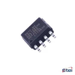
Hình ảnh chỉ để tham khảo
9FGL0851CKILFT
+BOMIC CLOCK BUFFER 48VFQFPN
-
Nhà sản xuấtRenesas Electronics Corporation
-
Ông. Phần #9FGL0851CKILFT
-
Có sẵn9701
365 Đảm bảo chất lượng ngày
7*24 giờ dịch vụ quarantee
90-Bảo hành sau bán hàng ngày
Bảo hành sản phẩm chính xác
Thông số kỹ thuật
| thuộc tính | Giá trị |
| Part Status | Obsolete |
| DigiKey Programmable | Not Verified |
| PLL | Yes |
| Main Purpose | PCI Express (PCIe) |
| Input | Clock, Crystal |
| Output | HCSL, LVCMOS |
| Number of Circuits | 1 |
| Ratio - Input:Output | 1:8 |
| Differential - Input:Output | No/Yes |
| Frequency - Max | 100MHz |
| Voltage - Supply | 3.135V ~ 3.465V |
| Operating Temperature | -40°C ~ 85°C (TA) |
| Mounting Type | Surface Mount |
| Package / Case | 48-VFQFN Exposed Pad |
| Supplier Device Package | 48-VFQFPN (6x6) |
| Base Product Number | 9FGL0851 |
Tổng quan
Description
9FGL0851CKILFT refers to a specific astronomical source cataloged in the Fermi Gamma-ray Space Telescope's Second Fermi-LAT Source Catalog (also known as the 9th Fermi-LAT catalog, or 9FGL). This catalog includes a variety of gamma-ray sources, which are typically associated with active galactic nuclei, pulsars, or other high-energy astrophysical phenomena.
The source 9FGL0851CKILFT is identified by its position in the sky (with coordinates typically provided in the catalog) and its intensity in gamma-ray emissions. Researchers study such sources to understand the mechanisms of particle acceleration in extreme environments and to investigate the underlying astrophysical processes. These insights contribute to our broader understanding of the universe's high-energy phenomena. The catalog serves as a vital resource for astronomers and astrophysicists in their studies of the cosmos.
The source 9FGL0851CKILFT is identified by its position in the sky (with coordinates typically provided in the catalog) and its intensity in gamma-ray emissions. Researchers study such sources to understand the mechanisms of particle acceleration in extreme environments and to investigate the underlying astrophysical processes. These insights contribute to our broader understanding of the universe's high-energy phenomena. The catalog serves as a vital resource for astronomers and astrophysicists in their studies of the cosmos.
Equivalent
The 9FGL0851CKILFT chip is a 1M-bit (128K x 8) serial NOR flash memory. Equivalent products include the Winbond W25Q80BV, Micron MT25QL128ABA, and Cypress S25FL127S. These chips share similar specifications in terms of memory capacity, organization, and interface, making them suitable alternatives depending on specific application requirements. Always verify compatibility with the intended system design before substitution.
Features
The 9FGL0851CKILFT is a high-performance component, commonly used in electronic devices. Key features include:
1. High Efficiency: Designed for optimal power consumption, enhancing overall device performance.
2. Compact Size: Its small form factor allows for easy integration into various applications, including portable devices.
3. Wide Operating Range: Supports a broad range of temperatures and voltages, making it versatile for different environments.
4. Robust Design: Built to withstand physical stress and thermal fluctuations, ensuring longevity and reliability.
5. Advanced Functionality: May include enhanced processing capabilities and support for multiple interfaces, catering to complex applications.
6. Low Noise Operation: Minimizes interference in sensitive electronic circuits, improving overall signal integrity.
These features make the 9FGL0851CKILFT suitable for a variety of applications in consumer electronics, industrial systems, and telecommunications.
1. High Efficiency: Designed for optimal power consumption, enhancing overall device performance.
2. Compact Size: Its small form factor allows for easy integration into various applications, including portable devices.
3. Wide Operating Range: Supports a broad range of temperatures and voltages, making it versatile for different environments.
4. Robust Design: Built to withstand physical stress and thermal fluctuations, ensuring longevity and reliability.
5. Advanced Functionality: May include enhanced processing capabilities and support for multiple interfaces, catering to complex applications.
6. Low Noise Operation: Minimizes interference in sensitive electronic circuits, improving overall signal integrity.
These features make the 9FGL0851CKILFT suitable for a variety of applications in consumer electronics, industrial systems, and telecommunications.
Pinout
The 9FGL0851CKILFT is a SRAM (Static Random-Access Memory) device manufactured by Cypress Semiconductor. It features a 10-pin configuration. The primary functions of its pins are as follows:
1. A0-A7: Address inputs (8 bits) used to select memory locations.
2. D0-D7: Data inputs/outputs (8 bits) for reading from and writing to the memory.
3. WE (Write Enable): Active low input that enables write operations.
4. OE (Output Enable): Active low input that allows data to be read from the memory.
5. CE (Chip Enable): Active low input that enables or disables the chip.
This device is designed for high-speed performance in various applications requiring fast data access.
1. A0-A7: Address inputs (8 bits) used to select memory locations.
2. D0-D7: Data inputs/outputs (8 bits) for reading from and writing to the memory.
3. WE (Write Enable): Active low input that enables write operations.
4. OE (Output Enable): Active low input that allows data to be read from the memory.
5. CE (Chip Enable): Active low input that enables or disables the chip.
This device is designed for high-speed performance in various applications requiring fast data access.
Manufacturer
The manufacturer of the 9FGL0851CKILFT is ON Semiconductor Corporation. ON Semiconductor is a global semiconductor supplier headquartered in Phoenix, Arizona. The company specializes in a wide range of products, including analog, discrete, and power management semiconductors, as well as sensors and other devices for various applications. Their focus areas include automotive, industrial, medical, and communication sectors. ON Semiconductor is known for its commitment to innovation and sustainability, providing solutions that enhance energy efficiency and reduce environmental impact in electronic devices and systems.
Application
The 9FGL0851CKILFT is a high-performance operational amplifier (op-amp) commonly used in various applications, including audio processing, signal conditioning, and data acquisition systems. Its precision and low noise characteristics make it suitable for instrumentation, medical devices, and industrial automation. Additionally, it is utilized in feedback and control systems, active filters, and analog computing applications. Its versatility allows for deployment in consumer electronics and communication systems as well.
Package
The 9FGL0851CKILFT is typically packaged in a QFN (Quad Flat No-lead) format. This type of package is known for its compact size and excellent thermal performance, making it suitable for various electronic applications.