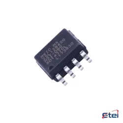
Hình ảnh chỉ để tham khảo
ADPA7001CHIPS
+BOM50 GHZ TO 90 GHZ 75 MW PA
-
Nhà sản xuấtCông ty Analog Devices Inc.
-
Ông. Phần #ADPA7001CHIPS
-
Bảng dữ liệu ADPA7001CHIPS DataSheet
-
Gói Die
-
Có sẵn25
365 Đảm bảo chất lượng ngày
7*24 giờ dịch vụ quarantee
90-Bảo hành sau bán hàng ngày
Bảo hành sản phẩm chính xác
Thông số kỹ thuật
| thuộc tính | Giá trị |
| Supplier | Analog Devices Inc. |
| Package | Tray |
| ProductStatus | Active |
| Frequency | 50GHz ~ 95GHz |
| P1dB | 17.5dBm |
| Gain | 14.5dB |
| RFType | General Purpose |
| Voltage-Supply | 1.5V ~ 4V |
| Current-Supply | 350mA |
| TestFrequency | 70GHz ~ 90GHz |
| MountingType | Surface Mount |
| Package/Case | Die |
Tổng quan
Description
1. Course Objectives: Provide an in-depth understanding of advanced data processing techniques or semiconductor technology, depending on the context.
2. Curriculum: Cover topics such as chip design, fabrication, data analytics, and emerging technologies in the semiconductor industry.
3. Target Audience: Intended for students, researchers, or professionals seeking advanced knowledge in the subject matter.
4. Learning Outcomes: Equip participants with the skills necessary to innovate and solve complex problems in related fields.
For specific details, including course content, prerequisites, and assessment methods, it would be best to consult the course syllabus or contact the educational institution offering it.
Equivalent
1. QPA2213 by Qorvo: A power amplifier targeting similar frequency ranges.
2. TGA2222 by TriQuint (Qorvo): Offers similar functionality and frequency range.
3. HMC1087 by Analog Devices: Another GaAs pHEMT power amplifier option.
When selecting equivalents, consider the frequency range, gain, power output, and other specifications to match your application's requirements.
Features
1. High Frequency Range: The amplifier operates over a wide frequency range from 2 GHz to 50 GHz, making it suitable for various applications in broadband systems.
2. High Gain: It provides a typical gain of 12 dB, ensuring strong signal amplification.
3. Output Power: The amplifier offers a typical output power of 20 dBm at 1 dB compression point, enabling it to handle significant signal levels.
4. High Linearity: With an output third-order intercept (IP3) of 28 dBm, it ensures excellent linearity and performance in multi-tone conditions.
5. Small Signal Gain Flatness: The gain flatness is typically ±1 dB across the entire bandwidth, ensuring consistent performance over its operating frequency range.
6. Compact Size: The chip form factor allows for easy integration into compact systems.
7. Supply Voltage: It operates from a typical supply voltage of 5 V, balancing performance and power consumption.
These features make it suitable for applications in military, aerospace, test equipment, and communications systems.
Pinout
1. RF Input (RFIN): This pin is used for the RF input signal. The signal enters the chip here to be amplified.
2. RF Output (RFOUT): This pin is where the amplified RF signal is outputted. It directs the signal after amplification for further use in the circuit or system.
3. Drain Bias (VDD): This pin provides the necessary DC voltage for the drain of the amplifier transistors. Proper biasing is crucial for optimal performance.
4. Gate Bias (VGG): This pin is used to supply the gate voltage required to set the operating point of the transistors and control the biasing condition.
5. Ground (GND): This pin connects the chip to ground, providing a reference point for the circuit and ensuring stable operation.
Please refer to the official datasheet for detailed specifications and recommended operating conditions.