
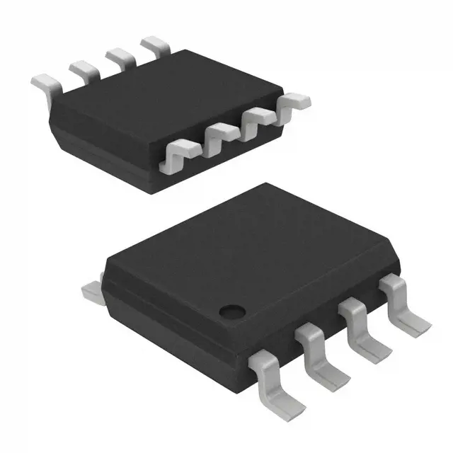
Hình ảnh chỉ để tham khảo
FDS4953
+BOMMOSFET 2P-CH 30V 5A 8SOIC
-
Nhà sản xuấtonsemi
-
Ông. Phần #FDS4953
-
Bảng dữ liệu FDS4953 DataSheet
-
Có sẵn8731
365 Đảm bảo chất lượng ngày
7*24 giờ dịch vụ quarantee
90-Bảo hành sau bán hàng ngày
Bảo hành sản phẩm chính xác
Thông số kỹ thuật
| thuộc tính | Giá trị |
| Series | PowerTrench® |
| Part Status | Obsolete |
| Base Product Number | FDS49 |
| Technology | MOSFET (Metal Oxide) |
| Configuration | 2 P-Channel (Dual) |
| FET Feature | Logic Level Gate |
| Drain to Source Voltage (Vdss) | 30V |
| Current - Continuous Drain (Id) @ 25°C | 5A |
| Rds On (Max) @ Id, Vgs | 55mOhm @ 5A, 10V |
| Vgs(th) (Max) @ Id | 3V @ 250µA |
| Gate Charge (Qg) (Max) @ Vgs | 9nC @ 5V |
| Input Capacitance (Ciss) (Max) @ Vds | 528pF @ 15V |
| Power - Max | 900mW |
| Operating Temperature | -55°C ~ 175°C (TJ) |
| Mounting Type | Surface Mount |
| Package / Case | 8-SOIC (0.154", 3.90mm Width) |
| Supplier Device Package | 8-SOIC |
| Packaging | Tape & Reel (TR) |
Tổng quan
Description
Students can expect to engage in research projects, case studies, and hands-on activities that enhance their understanding of food systems and dietary practices. The course aims to prepare students for careers in food industry, nutrition consulting, or further academic pursuits.
Key outcomes often include the ability to critically analyze food-related issues, develop innovative food products, and implement safety regulations. Overall, FDS4953 serves as a capstone experience, integrating various aspects of food science and nutrition to equip students with the necessary skills for professional success.
Equivalent
Features
1. Core Architecture: Based on a 32-bit architecture, offering improved processing power and efficiency.
2. Memory Capacity: Typically includes a combination of flash memory and RAM, allowing for flexible application development.
3. Integrated Peripherals: Equipped with various interfaces such as UART, SPI, I2C, and GPIOs, facilitating connectivity with other devices.
4. Low Power Consumption: Designed for battery-operated devices, featuring sleep modes to extend battery life.
5. Analog Features: Often includes ADCs and DACs for signal processing in sensor applications.
6. Development Support: Compatible with popular development environments and IDEs, ensuring ease of use for developers.
7. Security Features: May incorporate encryption and secure boot capabilities to protect sensitive data.
These features make the FDS4953 suitable for applications in IoT, consumer electronics, and industrial automation.
Pinout
Pin Functions:
1. Gate 1 (G1): Controls the switching of the first N-channel MOSFET.
2. Drain 1 (D1): The drain terminal of the first N-channel MOSFET.
3. Source 1 (S1): The source terminal of the first N-channel MOSFET.
4. Gate 2 (G2): Controls the switching of the second N-channel MOSFET.
5. Drain 2 (D2): The drain terminal of the second N-channel MOSFET.
6. Source 2 (S2): The source terminal of the second N-channel MOSFET.
These MOSFETs are typically used in applications such as load switching, power management, and DC-DC converters due to their low on-resistance and efficient switching capabilities. Always refer to the specific datasheet for detailed electrical characteristics and ratings.
Manufacturer
Application
1. Pharmaceuticals: Serving as a precursor in drug synthesis and development.
2. Agricultural Chemicals: Used in the formulation of agrochemicals for pest control.
3. Polymer Science: As a building block in creating specialty polymers and resins.
4. Electronics: Incorporated in the production of electronic materials and devices.
5. Cosmetics: Utilized in formulations for personal care products.
Overall, FDS4953 plays a significant role in various industries, enhancing product performance and functionality.
Package
Frequently Asked Questions
Q: What is the maximum drain-source voltage for the FDS4953?
A: The maximum drain-source voltage (Vdss) is 30V, suitable for low-voltage power management circuits.
Q: Can this MOSFET handle continuous current at 25°C?
A: Yes, the continuous drain current (Id) is rated at 5A at 25°C ambient temperature.
Q: What is the typical Rds(on) for this logic-level gate MOSFET?
A: The maximum Rds(on) is 55mOhm at Vgs=10V and Id=5A, ensuring low conduction losses.
Q: What is the gate charge requirement for switching applications?
A: The maximum gate charge (Qg) is 9nC at Vgs=5V, enabling fast switching in high-frequency designs.
Q: What is the maximum power dissipation for the FDS4953?
A: The maximum power dissipation is 900mW, requiring careful thermal management in the 8-SOIC package.
Q: Does this component support surface mount assembly?
A: Yes, it comes in an 8-SOIC surface mount package, suitable for automated PCB assembly processes.


