
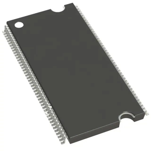
Hình ảnh chỉ để tham khảo
MT48LC4M32B2TG-7:G
+BOMIC DRAM 128MBIT PAR 86TSOP II
-
Nhà sản xuấtMicron Technology Inc.
-
Ông. Phần #MT48LC4M32B2TG-7:G
-
Có sẵn9186
365 Đảm bảo chất lượng ngày
7*24 giờ dịch vụ quarantee
90-Bảo hành sau bán hàng ngày
Bảo hành sản phẩm chính xác
Thông số kỹ thuật
| thuộc tính | Giá trị |
| Part Status | Obsolete |
| Base Product Number | MT48LC4M32B2 |
| DigiKey Programmable | Not Verified |
| Memory Type | Volatile |
| Memory Format | DRAM |
| Technology | SDRAM |
| Memory Size | 128Mbit |
| Memory Organization | 4M x 32 |
| Memory Interface | Parallel |
| Clock Frequency | 143 MHz |
| Write Cycle Time - Word, Page | 14ns |
| Voltage - Supply | 3V ~ 3.6V |
| Operating Temperature | 0°C ~ 70°C (TA) |
| Mounting Type | Surface Mount |
| Package | 86-TFSOP (0.400", 10.16mm Width) |
| Supplier Device Package | 86-TSOP II |
| Packaging | Tray |
| Access Time | 5.5 ns |
Tổng quan
Description
Equivalent
1. Hynix H5TQ4G83EFR-PBA
2. Samsung K4B4G0832F-BCH9
3. Micron MT41K256M16HA-125
4. Nanya NT5CB256M16DP-DI
Always verify compatibility based on specifications like voltage, speed, and package type before substituting.
Features
1. Capacity: 1 Gigabit (Gb) storage, organized as 4 banks of 32 bits each.
2. Data Rate: Operates at a speed of 1600 MT/s (million transfers per second).
3. Voltage: Low operating voltage of 1.5V, with a maximum of 1.575V.
4. Package: Available in a 78-ball TFBGA package, facilitating compact design in various applications.
5. Temperature Range: Industrial temperature range (-40°C to +95°C).
6. Latency: Supports CAS latency options of 7, 8, and 9.
7. Compatibility: Designed to be compatible with DDR3 standards, making it suitable for use in laptops, desktops, and other computing devices.
8. Features: Includes features like self-refresh, power-saving modes, and burst modes for improved performance and energy efficiency.
This makes it a reliable choice for high-performance memory applications.
Pinout
Key pins include:
- DQ0-DQ31: Data input/output pins for data transfer.
- A0-A11: Address pins for row and column selection.
- BA0-BA1: Bank address pins for selecting the memory bank.
- CLK: Clock input for synchronizing operations.
- CS: Chip select for enabling the chip.
- WE: Write enable for data writing operations.
- CAS: Column address strobe for read operations.
- RAS: Row address strobe for activating the row.
This chip is designed for various applications requiring high-speed memory access.
Manufacturer
Micron operates in the semiconductor industry, focusing on innovation in memory technology to meet the growing demands of data-intensive applications. The company is recognized for its commitment to research and development, enabling advancements in memory technology that enhance performance, efficiency, and reliability. Micron is one of the largest manufacturers of DRAM and NAND memory globally, serving diverse markets and contributing significantly to the evolution of digital technologies.
Application
Package
Frequently Asked Questions
Q: What is the memory density and organization of the MT48LC4M32B2TG-7:G?
A: It is a 128Mbit SDRAM, organized as 4M x 32 bits, ideal for 32-bit bus applications.
Q: What is the maximum clock frequency supported by this DRAM?
A: It supports a maximum clock frequency of 143 MHz, enabling high-speed synchronous operation.
Q: What is the typical access time for this SDRAM?
A: The access time is 5.5 ns, ensuring fast data retrieval for time-sensitive tasks.
Q: What voltage supply does the MT48LC4M32B2 require?
A: It operates with a supply voltage range of 3V to 3.6V, compatible with standard 3.3V logic.
Q: What is the write cycle time for this device?
A: The write cycle time for word and page operations is 14ns, supporting efficient data writing.
Q: Is this component suitable for surface-mount assembly?
A: Yes, it comes in a surface-mount 86-TSOP II package, facilitating automated PCB assembly.
Q: What is the operating temperature range of this memory?
A: It operates from 0°C to 70°C (TA), making it suitable for commercial-grade environments.





