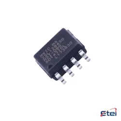
Hình ảnh chỉ để tham khảo
NCE3095K
+BOM-
Nhà sản xuấtWuxi NCE Power Semiconductor
-
Ông. Phần #NCE3095K
-
Có sẵn7705
365 Đảm bảo chất lượng ngày
7*24 giờ dịch vụ quarantee
90-Bảo hành sau bán hàng ngày
Bảo hành sản phẩm chính xác
Thông số kỹ thuật
| thuộc tính | Giá trị |
| Manufacturer | Wuxi NCE Power Semiconductor |
| Package / Case | TO-252-2 |
| Operating Temperature | -55℃~+175℃ |
| Rds(on) | 5.1mΩ@10V,20A |
| Drain to Source Voltage (Vdss) | 30V |
| Pd - Power Dissipation | 95W |
| Current - Continuous Drain(Id) | 95A |
| Reverse Transfer Capacitance (Crss @ Vds) | 212pF |
| Input Capacitance(Ciss @ Vds) | 1.784nF@15V |
| Type | 1 N-channel |
| Gate Threshold Voltage (Vgs(th) @ Id) | 2.2V |
| Gate Charge(Qg) | 38.4nC@15V |
Tổng quan
Description
NCE3095K is a high-performance, dual N-channel MOSFET designed for various power management applications. It features low on-resistance and fast switching capabilities, making it suitable for use in power supplies, motor drivers, and DC-DC converters. The device operates at a wide range of voltages and is capable of handling high currents, ensuring efficient operation in demanding environments.
The NCE3095K typically comes in a compact package, which facilitates easy integration into circuit designs while minimizing space. Its thermal performance is optimized for effective heat dissipation, ensuring reliable operation under high load conditions.
Key specifications include a maximum drain-source voltage (VDS) and a low gate threshold voltage (VGS) that enhances its drive characteristics. Overall, the NCE3095K is ideal for engineers seeking reliable, efficient solutions for modern electronic devices requiring robust power management.
The NCE3095K typically comes in a compact package, which facilitates easy integration into circuit designs while minimizing space. Its thermal performance is optimized for effective heat dissipation, ensuring reliable operation under high load conditions.
Key specifications include a maximum drain-source voltage (VDS) and a low gate threshold voltage (VGS) that enhances its drive characteristics. Overall, the NCE3095K is ideal for engineers seeking reliable, efficient solutions for modern electronic devices requiring robust power management.
Equivalent
The NCE3095K chip is a high-performance power management IC. Equivalent products include the LM2596 from Texas Instruments, MP1584 from Monolithic Power Systems, and the MIC2941 from Microchip Technology. Always verify specifications like voltage, current rating, and package type to ensure compatibility with your application.
Features
The NCE3095K is a high-performance N-channel MOSFET designed for various applications in power management and switching. Key features include:
1. Low On-Resistance (RDS(on)): Provides efficient power conduction and minimizes heat generation.
2. High Voltage Rating: Typically supports voltage levels up to 30V, making it suitable for various applications.
3. Fast Switching Speed: Enhances performance in high-frequency applications, aiding in efficient energy conversion.
4. Low Gate Charge (Qg): Reduces driver loss, improving overall efficiency in switching applications.
5. Thermal Stability: Designed to operate effectively across a wide temperature range, ensuring reliability under various conditions.
6. Applications: Commonly used in DC-DC converters, motor drivers, and power management systems.
These features make the NCE3095K a versatile choice for engineers seeking reliable and efficient MOSFET solutions.
1. Low On-Resistance (RDS(on)): Provides efficient power conduction and minimizes heat generation.
2. High Voltage Rating: Typically supports voltage levels up to 30V, making it suitable for various applications.
3. Fast Switching Speed: Enhances performance in high-frequency applications, aiding in efficient energy conversion.
4. Low Gate Charge (Qg): Reduces driver loss, improving overall efficiency in switching applications.
5. Thermal Stability: Designed to operate effectively across a wide temperature range, ensuring reliability under various conditions.
6. Applications: Commonly used in DC-DC converters, motor drivers, and power management systems.
These features make the NCE3095K a versatile choice for engineers seeking reliable and efficient MOSFET solutions.
Pinout
The NCE3095K is a high-voltage MOSFET that typically comes in a TO-220 package with a pin count of 3. The pin functions are as follows:
1. Gate (G): This pin is used to control the MOSFET. A voltage applied here enables or disables the current flow between the drain and source.
2. Drain (D): This pin is where the load is connected. The current flows from the drain to the source when the MOSFET is turned on (conducting state).
3. Source (S): This pin is connected to ground or the negative side of the circuit, serving as the return path for the current flowing through the device.
The NCE3095K is designed for applications requiring high efficiency, such as power supplies and motor drives.
1. Gate (G): This pin is used to control the MOSFET. A voltage applied here enables or disables the current flow between the drain and source.
2. Drain (D): This pin is where the load is connected. The current flows from the drain to the source when the MOSFET is turned on (conducting state).
3. Source (S): This pin is connected to ground or the negative side of the circuit, serving as the return path for the current flowing through the device.
The NCE3095K is designed for applications requiring high efficiency, such as power supplies and motor drives.
Manufacturer
The NCE3095K is manufactured by NCE Power Semiconductor, a company that specializes in the design and production of power semiconductor devices. NCE Power Semiconductor focuses on providing high-performance power electronic solutions, including transistors, diodes, and integrated circuits used in various applications like power management, motor control, and renewable energy systems. The company is known for its commitment to innovation and quality, catering to industries such as automotive, consumer electronics, industrial equipment, and telecommunications. NCE Power Semiconductor aims to deliver reliable and efficient products that meet the growing demands of modern electronic systems.
Application
NCE3095K is primarily used in power management applications, particularly in the fields of consumer electronics, telecommunications, and industrial equipment. Its high efficiency and low standby power consumption make it suitable for use in DC-DC converters, LED drivers, and power supplies. Additionally, it can be utilized in battery management systems for electric vehicles and renewable energy systems, helping to optimize energy usage and prolong battery life. Its versatility allows integration into various devices requiring efficient power conversion and regulation.
Package
The NCE3095K is typically available in a TO-220 package type. This package is known for its robust thermal performance and is commonly used in power transistors and regulators.