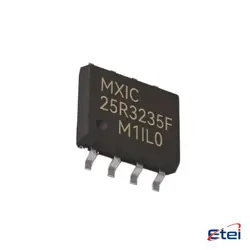
Hình ảnh chỉ để tham khảo
PCA9617ADPJ
+BOMIC REDRIVER I2C 1CH 1MHZ 8TSSOP
-
Nhà sản xuấtNXP Hoa Kỳ Inc.
-
Ông. Phần #PCA9617ADPJ
-
Bảng dữ liệu PCA9617ADPJ DataSheet
-
Gói SOT505-1
-
Có sẵn3924
365 Đảm bảo chất lượng ngày
7*24 giờ dịch vụ quarantee
90-Bảo hành sau bán hàng ngày
Bảo hành sản phẩm chính xác
Thông số kỹ thuật
| thuộc tính | Giá trị |
| Package | Tape & Reel (TR),Cut Tape (CT),Bulk |
| ProductStatus | Active |
| Type | Buffer, ReDriver |
| Applications | I²C |
| Input | 2-Wire Bus |
| Output | 2-Wire Bus |
| DataRate(Max) | 1MHz |
| NumberofChannels | 1 |
| Capacitance-Input | 10 pF |
| Voltage-Supply | 2.7V ~ 5.5V |
| Current-Supply | 8µA |
| OperatingTemperature | -40°C ~ 85°C |
| MountingType | Surface Mount |
| Package/Case | 8-TSSOP, 8-MSOP (0.118, 3.00mm Width) |
Tổng quan
Description
Key features include support for fast-mode plus (Fm+) I2C speeds up to 1 MHz, ensuring high-speed data transfer. Its unique architecture prevents latch-up and reduces ground bounce, enhancing reliability. The device also provides level shifting capabilities, bridging devices operating at different logic levels. It's often used in consumer electronics, industrial control systems, and communication devices where stable and efficient data transfer is critical. The PCA9617ADPJ is encapsulated in a small, 8-pin TSSOP package, offering a compact solution for complex electronic systems.
Equivalent
Features
Key features include:
- Dual bidirectional buffer for I²C-bus and SMBus.
- Level shifting capabilities between different voltage levels.
- Supports data transfer up to 1 MHz.
- Low standby current.
- Active-high enable pin to disable the buffer when not in use, saving power.
- ESD protection for enhanced reliability.
- Compact TSSOP package for space-constrained applications.
The PCA9617ADPJ is suitable for applications requiring buffering and level translation, such as motherboard-to-daughterboard communication, or interfacing low-voltage microcontrollers with higher-voltage peripheral devices.
Pinout
Here is a brief description of the pin functions:
1. VCC(A) (Pin 1): Power supply voltage for side A.
2. SDAA (Pin 2): Serial data line for side A.
3. SCLA (Pin 3): Serial clock line for side A.
4. GND (Pin 4): Ground.
5. SCLB (Pin 5): Serial clock line for side B.
6. SDAB (Pin 6): Serial data line for side B.
7. VCC(B) (Pin 7): Power supply voltage for side B; typically higher than VCC(A) for level translation.
8. EN (Pin 8): Enable pin to activate the repeater function.
The device allows for voltage translation between the two sides, and the enable pin controls whether the repeater is active, allowing for bus segmentation and isolation when needed.