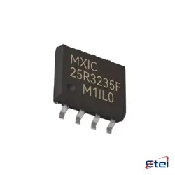
Hình ảnh chỉ để tham khảo
S29GL256P90FAIR10
+BOM-
Nhà sản xuấtInfineon / Cypress
-
Ông. Phần #S29GL256P90FAIR10
-
Có sẵn9301
365 Đảm bảo chất lượng ngày
7*24 giờ dịch vụ quarantee
90-Bảo hành sau bán hàng ngày
Bảo hành sản phẩm chính xác
Thông số kỹ thuật
| thuộc tính | Giá trị |
| Brand | Infineon / Cypress |
| Product Type | NOR Flash |
| Subcategory | Memory & Data Storage |
Tổng quan
Description
The S29GL256P90FAIR10 is a 256 Megabit (Mb) NOR Flash memory chip manufactured by Cypress Semiconductor. It is designed for high-performance embedded applications, offering fast read speeds of up to 90 ns, making it suitable for code execution and storage in systems requiring quick data retrieval. This device features a parallel interface, allowing for easy integration into various microcontroller and processor environments.
Key characteristics include a supply voltage range of 2.7V to 3.6V, enabling compatibility with low-power systems, and support for multiple programming and erase options, such as sector and chip erase. The S29GL256P also provides reliable data retention of up to 20 years and supports up to 100,000 program/erase cycles per sector. Its design includes advanced security features to protect against unauthorized access, making it ideal for applications in automotive, industrial, and consumer electronics. Overall, the S29GL256P90FAIR10 is a robust memory solution for developers looking for efficient and reliable data storage.
Key characteristics include a supply voltage range of 2.7V to 3.6V, enabling compatibility with low-power systems, and support for multiple programming and erase options, such as sector and chip erase. The S29GL256P also provides reliable data retention of up to 20 years and supports up to 100,000 program/erase cycles per sector. Its design includes advanced security features to protect against unauthorized access, making it ideal for applications in automotive, industrial, and consumer electronics. Overall, the S29GL256P90FAIR10 is a robust memory solution for developers looking for efficient and reliable data storage.
Equivalent
The S29GL256P90FAIR10 is a 256 Mb NOR Flash memory chip. Equivalent products include the Micron MT29F256G08CFAAA, Intel E28F256P30, and Spansion S29GL256N90TFI. Ensure compatibility with your specific application, focusing on voltage, interface, and timing specifications when selecting an equivalent.
Features
The S29GL256P90FAIR10 is a 256 Mb (32 MB) NOR Flash memory chip from Spansion. Key features include:
1. Memory Density: 256 Megabits, ideal for high-capacity applications.
2. Access Speed: 90 ns read access time, suitable for fast data retrieval.
3. Interface: 8-bit or 16-bit data bus, enabling flexible integration.
4. Programming Performance: Supports Byte, Word, and Page programming.
5. Erase Capability: Sector-based erasure (each sector is 64 KB), allowing targeted data management.
6. Endurance: Typically withstands 100,000 erase/program cycles, ensuring long-term reliability.
7. Data Retention: Maintains data integrity for over 20 years at 125°C.
8. Low Power Consumption: Features a low-power mode, enhancing battery life in portable devices.
9. Security: Includes features like hardware and software protection to safeguard data.
10. Temperature Range: Operates in an industrial temperature range, suitable for diverse applications.
This versatile Flash memory is widely used in embedded systems, automotive, and consumer electronics.
1. Memory Density: 256 Megabits, ideal for high-capacity applications.
2. Access Speed: 90 ns read access time, suitable for fast data retrieval.
3. Interface: 8-bit or 16-bit data bus, enabling flexible integration.
4. Programming Performance: Supports Byte, Word, and Page programming.
5. Erase Capability: Sector-based erasure (each sector is 64 KB), allowing targeted data management.
6. Endurance: Typically withstands 100,000 erase/program cycles, ensuring long-term reliability.
7. Data Retention: Maintains data integrity for over 20 years at 125°C.
8. Low Power Consumption: Features a low-power mode, enhancing battery life in portable devices.
9. Security: Includes features like hardware and software protection to safeguard data.
10. Temperature Range: Operates in an industrial temperature range, suitable for diverse applications.
This versatile Flash memory is widely used in embedded systems, automotive, and consumer electronics.
Pinout
The S29GL256P90FAIR10 is a 256 Mb (32 MB) NOR Flash memory chip from Cypress Semiconductor (now part of Infineon Technologies). It has a total of 48 pins.
Key functions of the pins include:
- Address Pins (A0-A21): Used to select memory locations.
- Data Pins (DQ0-DQ31): Bi-directional data lines used for data input and output.
- Control Pins:
- CE# (Chip Enable): Activates the memory chip.
- OE# (Output Enable): Controls data output.
- WE# (Write Enable): Enables writing to the memory.
- RESET#: Resets the chip.
- VCC: Power supply pin.
- VSS: Ground pin.
- WP# (Write Protect): Protects the memory from being written to.
- RY/BY# (Ready/Busy): Indicates the status of the memory operation.
This Flash memory is typically used in embedded systems for code storage and firmware updates.
Key functions of the pins include:
- Address Pins (A0-A21): Used to select memory locations.
- Data Pins (DQ0-DQ31): Bi-directional data lines used for data input and output.
- Control Pins:
- CE# (Chip Enable): Activates the memory chip.
- OE# (Output Enable): Controls data output.
- WE# (Write Enable): Enables writing to the memory.
- RESET#: Resets the chip.
- VCC: Power supply pin.
- VSS: Ground pin.
- WP# (Write Protect): Protects the memory from being written to.
- RY/BY# (Ready/Busy): Indicates the status of the memory operation.
This Flash memory is typically used in embedded systems for code storage and firmware updates.
Manufacturer
The S29GL256P90FAIR10 is manufactured by Spansion, which is a company known for producing flash memory solutions. Spansion specializes in NAND and NOR flash memory products used in a variety of applications, including consumer electronics, automotive, and industrial devices. The company was formed as a joint venture between AMD and Fujitsu, focusing on non-volatile memory solutions. Spansion has a reputation for innovation in memory technology, providing high-performance and reliable memory solutions for a wide range of markets.
Application
The S29GL256P90FAIR10 is a 256Mb NOR Flash memory chip used in various applications, including mobile and embedded systems. Key application areas include:
1. Consumer Electronics: Firmware storage in devices like smartphones, tablets, and digital cameras.
2. Automotive: Storing firmware for ECUs and infotainment systems.
3. Industrial: Data logging and firmware in industrial control systems and automation equipment.
4. Networking: Boot code and configuration storage in routers and switches.
5. IoT Devices: Firmware and application code for smart devices.
Its fast read speeds and reliability make it suitable for these diverse applications.
1. Consumer Electronics: Firmware storage in devices like smartphones, tablets, and digital cameras.
2. Automotive: Storing firmware for ECUs and infotainment systems.
3. Industrial: Data logging and firmware in industrial control systems and automation equipment.
4. Networking: Boot code and configuration storage in routers and switches.
5. IoT Devices: Firmware and application code for smart devices.
Its fast read speeds and reliability make it suitable for these diverse applications.
Package
The S29GL256P90FAIR10 is packaged in a 64-pin TSOP (Thin Small Outline Package) with a dimensions of 10mm x 14mm. This type of packaging is designed for surface mounting on PCBs, allowing for efficient space utilization and heat dissipation.