
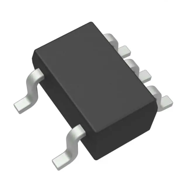
Hình ảnh chỉ để tham khảo
SN74AUC1G126DCKR
+BOMIC BUFF NON-INVERT 2.7V SC-70-5
-
Nhà sản xuấtTexas Dụng cụ
-
Ông. Phần #SN74AUC1G126DCKR
-
Bảng dữ liệu SN74AUC1G126DCKR DataSheet
-
Có sẵn2239
365 Đảm bảo chất lượng ngày
7*24 giờ dịch vụ quarantee
90-Bảo hành sau bán hàng ngày
Bảo hành sản phẩm chính xác
Thông số kỹ thuật
| thuộc tính | Giá trị |
| Series | 74AUC |
| Part Status | Active |
| Logic Type | Buffer, Non-Inverting |
| Number of Elements | 1 |
| Number of Bits per Element | 1 |
| Output Type | 3-State |
| Current - Output High, Low | 9mA, 9mA |
| Voltage - Supply | 0.8V ~ 2.7V |
| Operating Temperature | -40°C ~ 85°C (TA) |
| Mounting Type | Surface Mount |
| Package / Case | 5-TSSOP, SC-70-5, SOT-353 |
| Supplier Device Package | SC-70-5 |
| Base Product Number | 74AUC1G126 |
Tổng quan
Description
Key features include:
- Operates at a voltage range from 0.8V to 2.7V, making it suitable for low-voltage applications.
- High-speed operation with a typical propagation delay of 2.4 ns at 1.8V.
- Offers a 3-state output control, allowing for multiple devices on a single data line without interference.
- Low static and dynamic power consumption, contributing to efficient power management in portable and battery-operated devices.
- Available in a small SOT-353 package, ideal for space-constrained applications.
The SN74AUC1G126DCKR is widely used in computing, consumer electronics, and communication devices where space efficiency and high performance are critical.
Equivalent
1. Nexperia 74AUP1G126GW
2. ON Semiconductor NC7WZ126
3. Toshiba TC7WZ126FK
4. Fairchild NC7SZ126
Ensure compatibility in terms of package type, voltage, and other specifications. Always verify with the datasheets for exact equivalence.
Features
1. Low Power Consumption: Operates with a low power supply voltage range from 0.8 V to 2.7 V.
2. High-Speed Operation: Designed for high-speed applications with a maximum propagation delay of 2.5 ns at 1.8 V.
3. 3-State Output: Features an output-enable control that places the device in a high-impedance state, which allows for easy multiplexing.
4. Small Package: Available in a space-saving SC70-5 package, making it suitable for compact designs.
5. CMOS Technology: Built using advanced CMOS technology ensuring low power dissipation and high noise immunity.
6. Wide Temperature Range: Operates reliably in a wide temperature range from -40°C to 85°C.
7. Latch-Up Performance: Provides excellent latch-up immunity exceeding 100 mA per JESD 78, Class II.
This buffer/driver is ideal for applications requiring low voltage and high-speed data processing.
Pinout
The functions of the pins are as follows:
1. VCC - Power supply pin.
2. GND - Ground pin.
3. A - Input pin.
4. OE - Output enable pin (active-high). When high, the output is enabled. When low, the output is in a high-impedance state.
5. Y - Output pin, which follows the input state when OE is high.
The SN74AUC1G126DCKR is used in applications requiring a single buffer with a 3-state output, making it useful for signal isolation and multiplexing.


