
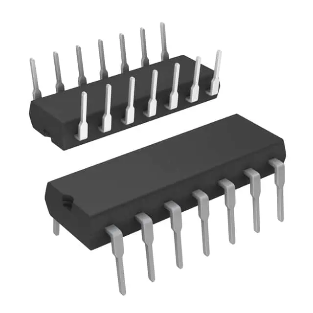
Hình ảnh chỉ để tham khảo
TLC556CN
+BOMIC OSC TIMER DUAL 2.1MHZ 14-DIP
-
Nhà sản xuấtTexas Dụng cụ
-
Ông. Phần #TLC556CN
-
Bảng dữ liệu TLC556CN DataSheet
-
Có sẵn6529
365 Đảm bảo chất lượng ngày
7*24 giờ dịch vụ quarantee
90-Bảo hành sau bán hàng ngày
Bảo hành sản phẩm chính xác
Thông số kỹ thuật
| thuộc tính | Giá trị |
| Supplier | Texas Instruments |
| Package | Tube |
| Series | LinCMOS™ |
| ProductStatus | Active |
| Type | 555 Type, Timer/Oscillator (Dual) |
| Frequency | 2.1MHz |
| Voltage-Supply | 2V ~ 18V |
| Current-Supply | 720 µA |
| OperatingTemperature | 0°C ~ 70°C |
| Package/Case | 14-DIP (0.300, 7.62mm) |
| SupplierDevicePackage | 14-PDIP |
Tổng quan
Description
The TLC556CN is known for its low power consumption, typically requiring less current than its bipolar counterparts, making it suitable for battery-powered devices. It operates over a wide supply voltage range, typically from 2 V to 15 V, and features low threshold and trigger currents, enhancing its versatility in various circuit designs. Additionally, it offers good temperature stability and a high degree of accuracy in its timing functions. These features make the TLC556CN a reliable choice for engineers looking to implement precise timing solutions in their electronic projects.
Equivalent
Features
1. Dual Timers: Contains two independent timing circuits, allowing for versatile applications.
2. Low Power Consumption: The CMOS technology ensures reduced power consumption compared to its bipolar counterparts.
3. Wide Supply Voltage Range: Operates from 2 V to 15 V, accommodating a variety of power supply conditions.
4. High Output Current: Can source or sink up to 100 mA, making it suitable for driving various loads.
5. Adjustable Duty Cycle: The design allows for a modifiable duty cycle, enabling flexibility in pulse-generation applications.
6. Low Standby Current: Offers low power draw in standby mode, improving efficiency in battery-powered devices.
7. Temperature Stability: Provides consistent performance over a wide temperature range.
Overall, the TLC556CN is well-suited for use in timing, pulse generation, and sequential timing applications, offering reliability and efficiency due to its CMOS construction.
Pinout
1. GND (Pin 7 & Pin 6): Ground reference voltage, connected to 0V.
2. VCC (Pin 14): Supply voltage, typically between 3V and 15V.
3. TRIG (Pin 2 & Pin 8): Trigger input, initiates the timing interval.
4. OUT (Pin 5 & Pin 9): Output pin, connected to the load.
5. RESET (Pin 4 & Pin 10): Resets the timer if held low.
6. CTRL (Pin 3 & Pin 11): Control voltage for adjusting the threshold and trigger levels.
7. THRES (Pin 6 & Pin 12): Threshold input, ends the timing interval.
8. DISCH (Pin 1 & Pin 13): Discharge pin, used to discharge the timing capacitor.
The TLC556CN can be used in applications such as monostable and astable multivibrators, pulse generation, and timing applications. Its dual nature allows for more compact and efficient designs requiring multiple timing operations.


